What is optical design and simulation? Off-the-shelf electromagnetic simulation software alone cannot meet the needs of customers in many cases. We offer optimal custom simulation services by combining conventional methods with our own proprietary methods.
Optical Simulation Services
Our experienced staff, who have been involved in the development of electromagnetic field simulators, can provide custom services to meet your needs.
Benefits to Customers: Optical Design/Simulation Services
It is possible to optimize our simulation software based on your objective
Avoid the need to purchase expensive software and computer workstations
Shorter design and product development cycles
No advanced expertise is required
Optical Design/Simulation Environment
SCIVAX has invested in computer system infrastructure to allow massive computer calculations needed for optical simulation
■ Hardware CPU Xeon 2.6GHz, Max 32 cores Memory 512GByte InfiniBand (High Speed Network) Connection
Optical Design/Simulation Services Flow
※ Based on structures involved and other factors, above flow may be altered.
Simulation Examples
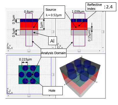
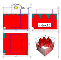
An example of improving LED external quantum efficiency by using microstructures formed on a sapphire substrate
The FDTD method has been used for various studies on external quantum efficiency simulations of LEDs, but it is not yet possible to optimize the microstructure due to the huge amount of calculation required. We have successfully simulated the external quantum efficiency of LEDs in a short period of time by combining the RCWA method with our original method.
We have confirmed that the simulation results are consistent with the actual external quantum efficiency measurement results using actual LED devices.
※SCIVAX has submitted a patent for this design
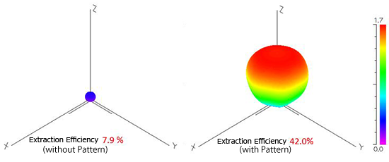
These are the simulation results of an LED element with the above structure. The diffraction efficiency is obtained by running multiple simulations under slightly different conditions. By post-processing the data, the extraction efficiency and light distribution are calculated.
Although the thickness of the structure in the example of simulation result 1 is 1.8 μm, it is possible to analyze even a thickness of 100 μm if the pattern is the same.
Simulation Result 1
LED Light Extraction Efficiency (RCWA Based)
Simulation Result 2
Simulation result 2 is the final output after post-processing.
The diffraction direction is the direction between the origin and the smallest polygon, and all diffraction efficiencies are shown in three dimensions.
Simulation Result 3
Simulations are performed with nanostructure geometry entered as parameters.
A model is constructed based on data verified with AFM, TEM and other nano-precise instruments.
Example of work with Meijo University regarding LED External Quantum Efficiency
SCIVAX is cooperating with Meijo University’s Professors Akasaki and Kamiyama to develop nano-patterned sapphire substrates (nPSS) based on collaboration in optical simulation and actual nPSS fabrication with the objective of improving LED light extraction efficiency.
Research Overview
Most patterned sapphire substrates (PSS) enable some improvement in LED light extraction, but the degree of improvement depends on the patterning geometry.
Also, the layered topography of grown crystalline layers must be accounted for in making judgements regarding optimal designs.
This research relies on both optical simulation and nanoimprint lithography technologies
Unprocessed
Nano-patterned
Simulation Example
The LED devices themselves and the nano-patterns which are hundreds of times smaller must be considered together, so FDTD simulation requires long calculation times and huge amounts of memory. As a result, limited range of simulations are possible to execute.
SCIVAX scientists realized that the periodic structure lent itself to combining the RCWA simulation method to generating a full 3D simulation and succeeded in producing the same.
This simulation was verified by Meijo Universities Professor Kamiyama’s model.
Unprocessed (Flat)
Nano-patterned (structured)
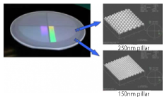
Patterning of Sapphire Substrates
It is possible to use NIL technology to pattern sapphire substrates.
Example of Moth-Eye Antireflection Structure
Moth-Eye and other nanostructures can be formed on reflective surfaces to significantly reduce surface reflectivity.
The anti-reflection performance is greatly affected by the geometry and materials of the nanostructures.
We can run continuous simulations with these conditions as parameters.
※We have confirmed that the simulation results are consistent with the measurement results using the actual device.
Simulation
Software Used: DiffractMOD (optical element analysis by the RCWA method)
Model Data (Refractive Index Distribution)
AFM Data Display
SEM Photo
Comparison to Actual Device Measurement
Measured Values
Simulation Result
Characteristics of SCIVAX's Originally Developed Ideal Moth-Eye Structure
Characteristics of SCIVAX's Originally Developed Ideal Moth-Eye Structure
Continuous simulation was performed with the shape of anti-reflective structures as a parameter.
It was possible to design and fabricate a master mold from the simulation model by creating a model from the AFM and TEM data of the anti-reflective structure.
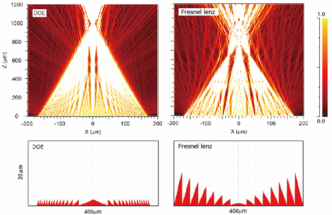
Example of Light Control Using DOE (Diffractive Optical Elements) Lens
Using a DOE lens, the direction of incident light, beam broadening angles, beam shape and focal length can be controlled.
SCIVAX can supply DOE lens technology from design to prototyping to volume production.
It is possible to control light distribution by modifying the repeating triangular patterns and distribution based on consideration of the diffraction angle and diffraction efficiency.
Regarding the simulation method
FDTD Method (Finite Difference Time Domain Method)
In this method, we breakdown space to a grid with a mesh pitch 1/10 of the launched wavelength, and the light propagates along with elapsed time. By applying the mesh grid, we can remove the quantum error and truly express Maxwell’s laws in the model.
When using this method, huge amounts of computer resource is required, so the simulation size will be limited to a few cubic microns with typical workstation.
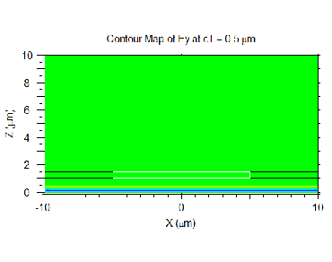
Below, using the FDTD method, we modelled the behavior of light in the case of a planewave with a wavelength of 0.5μm passing through 10μm and 0.5μm slits opened in a beam blocker. In the case of the small slit, the light propagates outward as a ripple. It has not been possible model light phenomena at this level with conventional tools. This requires analysis at the electromagnetic field level.
Behavior in the case of the 10μm slit in the blocker
Behavior in the case of the 0.5μm slit in the blocker
Using SCIVAX’s proprietary simulation methods, RCWA method simulations can be applied to larger dimension optical simulations.
RCWA Method (Rigorous Coupled Wave Analysis)
The RCWA method requires launching planewave, and also periodic boundary conditions (i.e. based on infinitely repeating identical patterns) should be applied. This method takes slices of the structural object in the vertical direction (i.e. optical axis), and performs a Fourier transformation on the distribution of refractive indices in each slice and performs calculations on these base data. If the refractive index distribution is also repeating, it is possible to take each slice as one chunk of data. Thus by taking advantage of the features of the RCWA method, simulations of devices in actual size can be done, and previously this has been impossible with the FDTD method.
Primary Output Data: Transmitted and reflected light’s diffractive efficiency (order of diffraction, diffraction angle, diffracted intensity)
※It makes sense that the total transmitted efficiency + the total reflected efficiency + the total absorption by structure = 1.