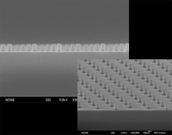
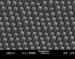
Pillar/Hole Pattern is used in various fields, such as improvement of LED external quantum efficiency, biosensor, metalens, metasurface, etc.
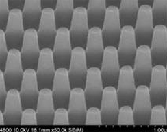
Pillar Pattern 1
φ100nm, Height 150nm
Pillar Pattern 2
φ230nm, Height 500nm (Silicon Wafer)
Pillar Pattern, formed on the sapphire wafer
Top Left: φ150nm,
Right: φ100nm,
Bottom Left: φ200nm,
Right: φ250nm
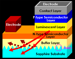
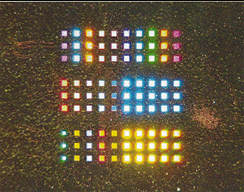
High Luminance LED Examples
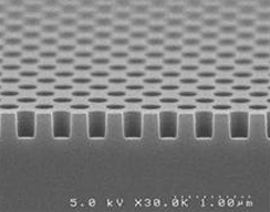
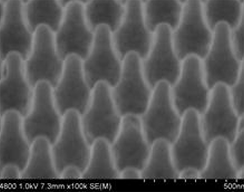
High Aspect Ratio Pillar Pattern
High Aspect Ratio(A/R=5)
Pillar Pattern
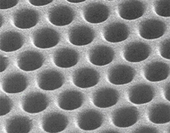
Hole Pattern 1
φ230nm Hole
Hole Pattern 2
φ230nm Hole, Magnified
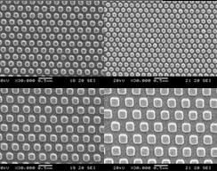
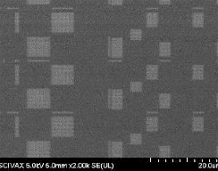
Semiconductor Isolated Pattern 1
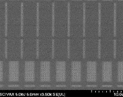
Semiconductor Isolated Pattern 2
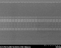
Semiconductor Isolated Pattern 3
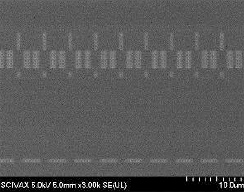
Semiconductor Isolated Pattern 4
Semiconductor Isolated Pattern 5
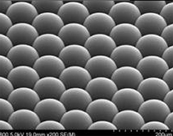
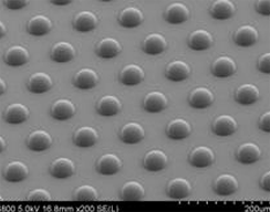
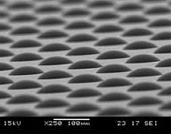
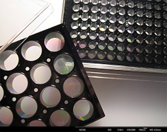
Lens Arrays
Lens arrays are being considered for use in a variety of optical devices.
Lens Arrays Pattern 1
Lens Arrays φ10μm~φ200μm
Lens Arrays Pattern 2
Lens Arrays φ10μm~φ200μm
Lens Arrays Pattern 3
Lens Arrays φ10μm~φ200μm
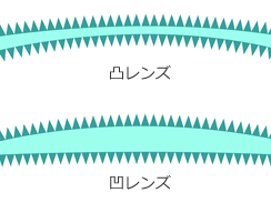
Anti-reflection Pattern
With Moth-Eye structure processing onto lens surfaces, some problems can be solved such as ghost, flare, etc.
Moth-Eye Structure1
Moth-Eye
Processing onto Lens Curved Surfaces
Moth-Eye Processing onto Lens Curved Surfaces.
Pitch 250nm~180nm
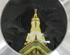
Unprocessed Lens
There is ghost image of photographer on the lens.
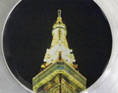
Moth-Eye Processed Lens for Both Surfaces
The image under the lens is clearly seen.
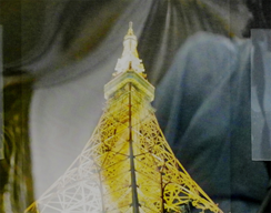
Unprocessed Film
Unprocessed Film
Moth-Eye Processed Film for Both Surfaces
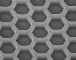
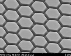
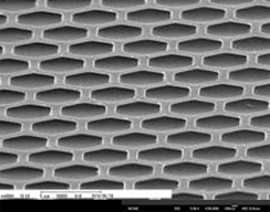
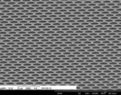
Honeycomb/Lattice Pattern
Honeycomb/Lattice Pattern is used for various fields, such as electronic materials, biology, etc.
Honeycomb Pattern 1
Width 100nm Honeycomb Pattern
Honeycomb Pattern 2
One side: 1μm~several tens of μm
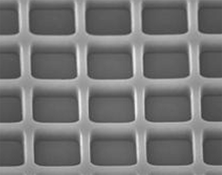
Square Pattern
One side: 1μm~several tens of μm
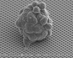
Cell Culture Plates Application
Three Dimensional Cell Culture Plates NanoCulture Plate
Cultured Cell
Form a spheroid in the patterned culture
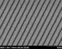
L&S Pattern
L&S Pattern can be fabricated in several tens of nm, practical application is in progress for various fields, such as polarizing plate for a liquid crystal panel.
L&S Pattern 1
Several tens of nm~a few hundreds of μm
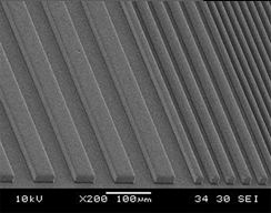
L&S Pattern 2
Several tens of nm~a few hundreds of μm
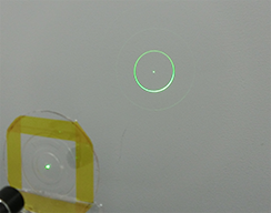
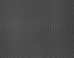
Photonic Crystal Application
Appearance of Optical Diffraction by DOE
Pattern for Optical Diffraction (Concentric Circles)
Metal Wiring
Metal Wiring practical application is in progress for various fields, such as touch panel.
Ag Thin Wire Pattern 1
Ag Thin Wire Pattern on PET Film (Linewidths: 50nm~1μm)
Ag Thin Wire Pattern 2
Ag Thin Wire Pattern on PET Film (Linewidths: 50nm~1μm)