Visual inspection is a very important elemental technology for the mass production of nanoimprint-based microfabrication.
We support our customers from prototyping to mass production based on a variety of inspection technologies, including a cutting-edge high-speed visual inspection system (INSPECTRA).
Metrology System Lineup
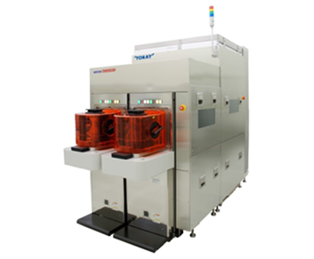
Wafer Inspection system: INSPECTRA
Primary Application: Automatic macro analysis of wafer or film surface
Primary Features & Options
Resolution
1.4μm、3.5μm
Magnification
2X or 5X
Minimum Detectable Defect:
2μm
Substrate Size:
Max 300mm square
Throughput (6" wafers):
about 50 wph
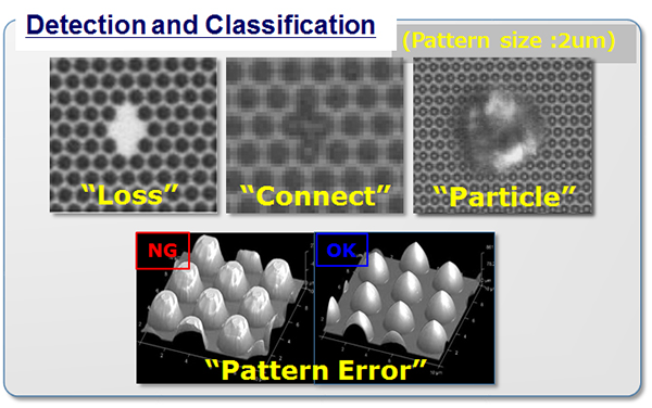
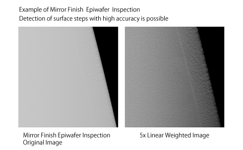
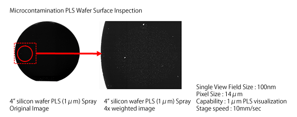
Inspection Examples
Details of Large Area Pattern Inspection System
System:
OPTOSCAN
Primary Applications:
●Features・・・using telocentric optics, micron order level pattern non-uniformity, micro-scratches, particles, resin non-uniformity can all be confirmed with high-speed
Primary Features:
Measurement area・・・~300mm□
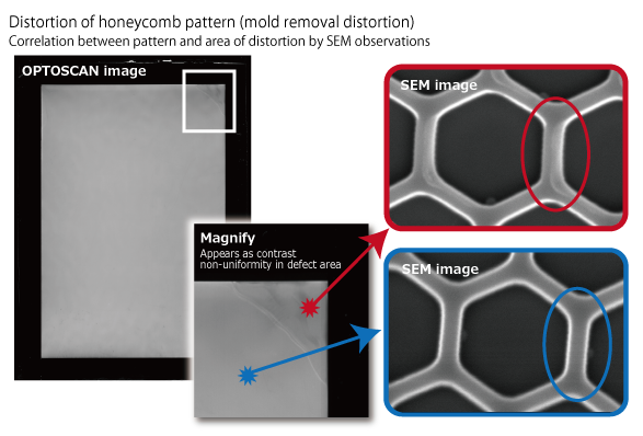
Large Area Nano-pattern Inspection System: OptoScan 700
The macro optical system can be used to evaluate molds and transfer films. It is possible to evaluate and inspect pattern defects and non-uniformity of the release agent coating in a short time by capturing the image of the pattern on the nanoimprint mold or transfer film in a macro view.
●Mold Evaluation and Analysis ●Various Pattern Geometries and Mold Materials (Ni, Fused Silica, resin, etc.) ●Monitoring of Release Agent Degradation and Film Delamination ●Evaluation and Analysis of Transferred Pattern Uniformity ●SCIVAX uses proprietary technology to achieve high speed and high sensitivity product imaging
Scanning Electron Microscope
Primary Applications:
Inspection of nanometer level patterns
Primary Features/Resolution:
1.3nm (imaging voltage 1kV)
Imaging Voltage Range:
0.1 to 30 kV
Magnification:
up to 2,000,000X
Atomic Force Microscope (AFM)
System Name:
Dimension Icon
Primary Applications & Features:
Can handle large area samples with its scanning probe microscopy function.
Primary Functions:
The system can measure pattern dimensions and step heights with atomic level resolution.
Film Reflectivity/Thickness Measurement Equipment
System Type:
NIR Microspectroscope
Primary Applications:
Features・・・Optically measures the reflectivity and thickness of film/patterns