SCIVAX Nanoimprint Foundry
(Nanoimprint Volume Production Services)
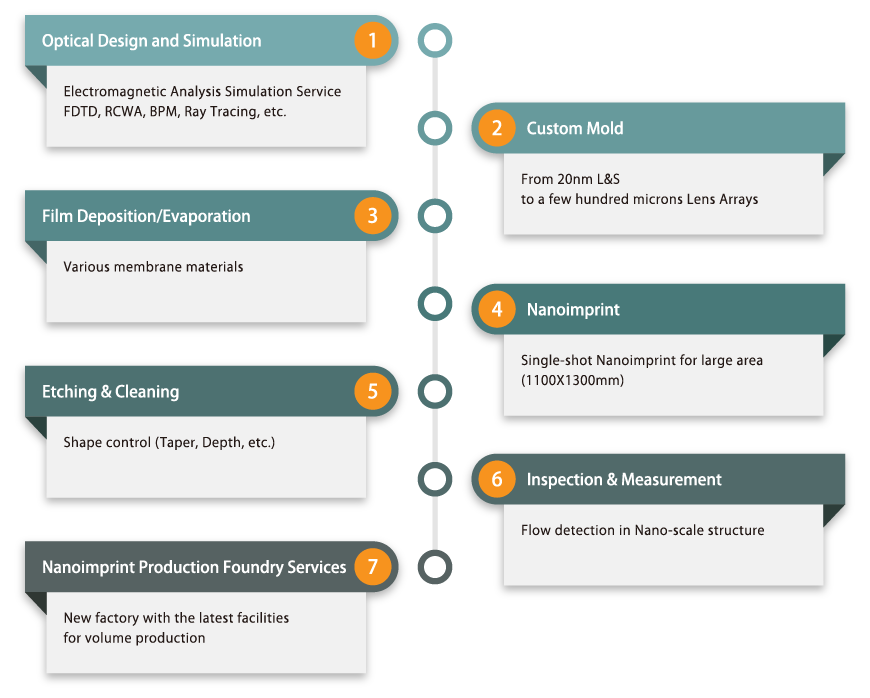
SCIVAX offers a one-stop solution for nano-patterning from basic optical simulation to volume production foundry services.
It is not possible to achieve mass production with nanoimprinting technology alone. We have developed a unique microfabrication foundry platform by combining it with peripheral technologies necessary for practical application. By using this foundry service, you will be able to drastically shorten the development period of your new products.
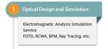
Optical Design and Simulation
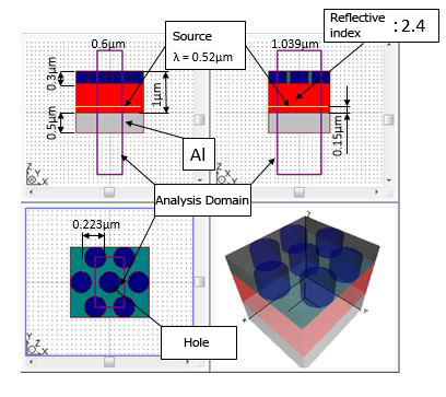
Off-the-shelf electromagnetic simulation software alone cannot meet the needs of customers in many cases.
We offer optimal custom simulation services by combining conventional methods with our own proprietary methods.
- Service Introduction
- Simulation Flow
- Examples
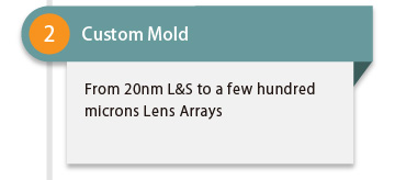
Custom Mold
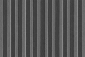
We can provide a variety of mold types to suit your needs, from small molds for R&D purposes to large molds for mass production.
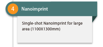
Nanoimprint
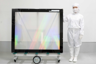
with SCIVAX’s unique single-shot NIL technology, nanoimprinting is possible for various substrates ranging from silicon substrates, compound semiconductor substrates to large glass substrates.
・Wafers(φ2″~φ12″)
・Glass Substrates (Maximum 1,100mmX1,300mm)
・Glass Lenses
・Metal Substrates
・All types of films/sheets and other substrates
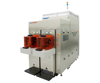
Inspection & Measurement
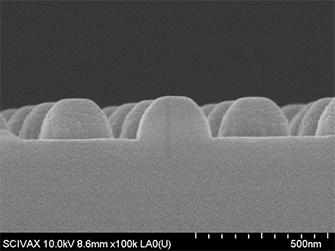
Various inspections are performed using high-precision inspection equipment.
Surface shape measurement, pattern defects and foreign matter can be inspected.
We also sell macro inspection systems.
- Low Cost Custom Molds
- Mixed Pattern Mold
- Large Area Molds
- Mold List
Nanoimprint Production Foundry Services
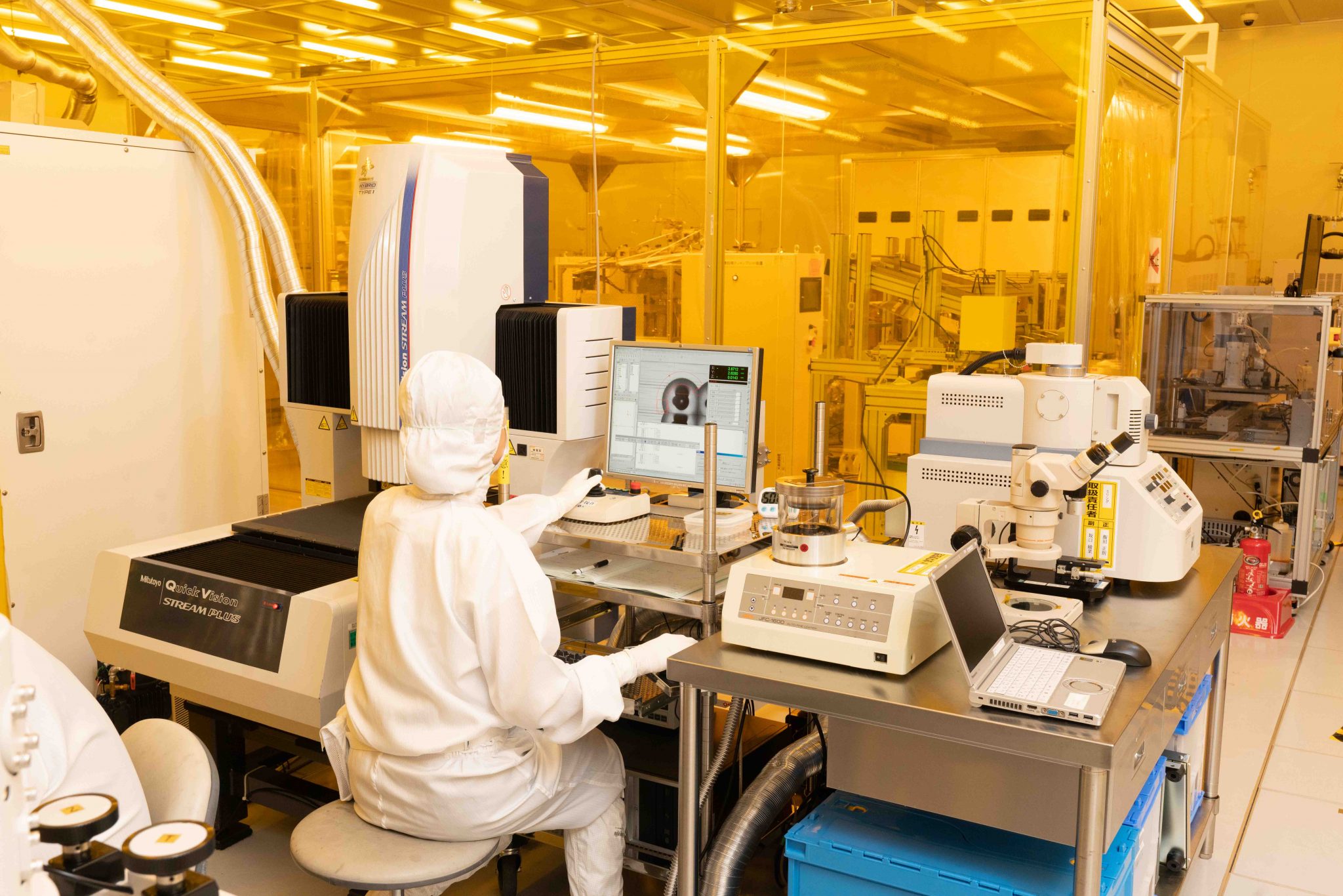
In order to conduct volume manufacturing for devices with nanostructures, a high level specification of environmental cleanliness and strict management of the same is a requirement. SCIVAX has established a manufacturing facility in Toyama Prefecture that features a state-of-the-art cleanroom.
- Volume Manufacturing

NANOBIC 7-7,
Shinkawasaki,
Saiwai-ku, Kawasaki City,
Kanagawa Prefecture
212-0032


