Etching & Cleaning
Do you have trouble with etching with nano-imprint resists? We can help you solve various dry-etching issues related to nano-imprinted resists.
Etched Films
We can handle substrate size, types of film to be etched, and various pattern sizes.
We can provide a full range of services from resist mask formation by nanoimprinting to etching optimization.
| ■Films that can be etched | ●Silicon ●SiOx ●Glass ●sapphire ●All types of metal layers ●All types of compound semiconductor layers |
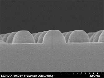
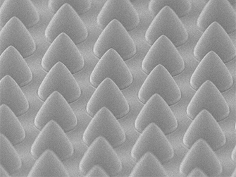
| ■Etching Geometries | ●Hole ●Pillar ●Line&Space ●Cones ●Other |
| Pattern Size | ●20nm~several tens of μm |
| ■Equipment | ●ICP & RIE Etchers |
Etching Method
Residual Layer Etching

The etching rate control solves the problem of residual film etching.
Thin resist

The problem of resist shortage is solved by controlling the etching selection ratio.
Etch Profile Control

Various shapes can be controlled.
Taper Etching

Etching Examples
Fused Silica Etching

Sapphire Etching

Etching Foundry Service Flow
SCIVAX is able to provide consulting services regarding etching processes. Please feel free to inquire.
Limited to etching of NIL processed substrates.
1.
2.
3.
4.
Confirmation of Specification
Technical Consulting
Job Quotation
Sample Production
① Confirmation of Specification
We will ask about the substrate and film type, as well as the shape, dimensions and accuracy to be used.
② Technical Consulting
We offer technical consulting regarding equipment, gases and process conditions.
③ Job Quotation
Step-by-step recommendations can be made to fit your budget.
④ Sample Production
We deliver high quality samples based on our extensive experience and high technology.

NANOBIC 7-7,
Shinkawasaki,
Saiwai-ku, Kawasaki City,
Kanagawa Prefecture
212-0032

