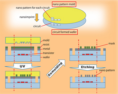
NOC Process
(Nanoimprint On Circuit wafer Process)
SCIVAX revolutionary NOC Process enables nanoimprint patterning on wafers with existing CMOS or circuit patterns.
・Alignment The global alignment accuracy across wafer (φ8”) is ±3μm ・Low shrinkage process Dimension control based on resin or mold shrinkage ・Curved surface patterning UV irradiation, Mold release, Etching Full surface patterning of substrates with a total warpage larger than 100μm is possible
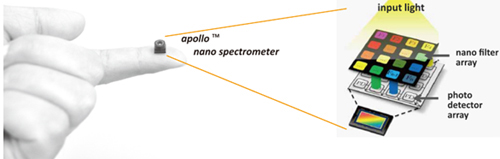
We have developed the world's smallest wavelength sensor (spectrometer) based on nano-patterned surface plasmon color filter arrays
What is a surface plasmon?
A vibration wave that propagates across a metal surface when the vibration of free electrons on the metal surface is coupled with light.
Technology based on surface plasmon is expected to enable many revolutionary devices in the IoT
apollo was developed by nanoLambda Corp., and is the world’s smallest wavelength sensor
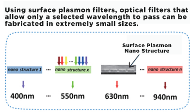
Principle of the surface plasmon filter
Using surface plasmons, it is possible to fabricate tiny filters that are transparent at any wavelength.