"Nanoimprint onto large area"
opens up the future of super
nanofabrication technology
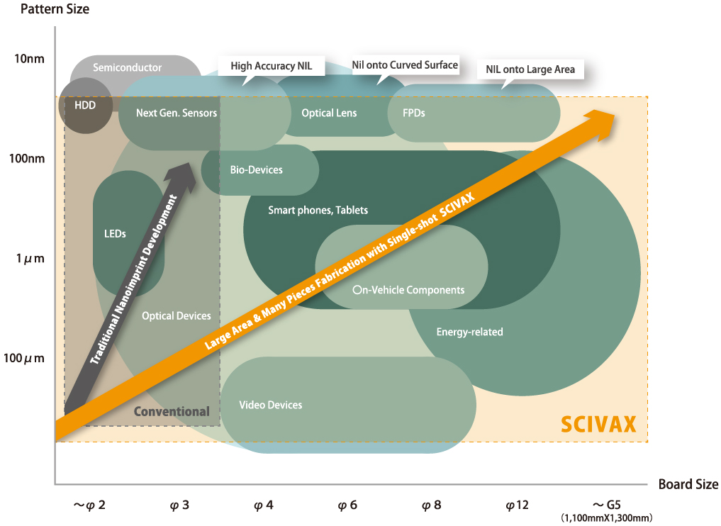
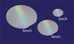
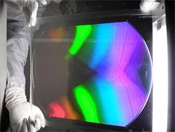
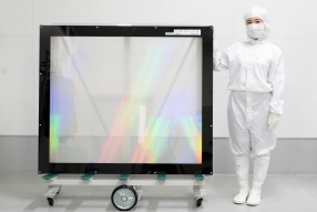
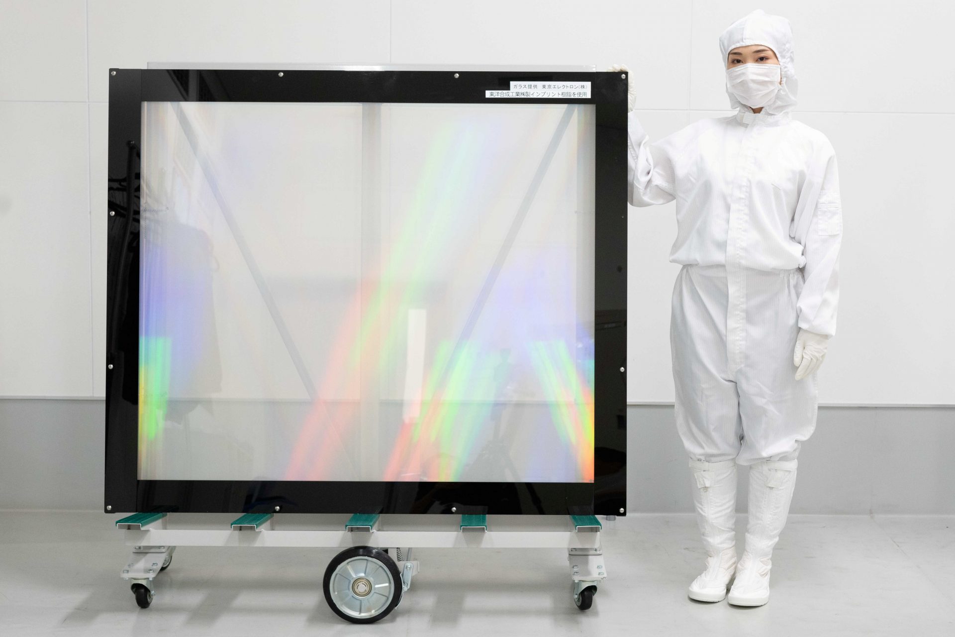
With our originally developed Large Area Nanoimprint Technology, the cost for processing can be drastically reduced, so it is spreading to various applications now. “For large area glass: single-shot fabrication on G5 (1,100mmX1,300mm)” and “For wafer fabrication: high throughput at most φ8 inches” can be done.
Nanoimprint Foundry Service
(Volume Production Service)
Only with Nanoimprint Technology, a volume production can’t be realized. We make an effort for the fusion technology which is required for practical application, then we have constructed our original Foundry Platform for nanoscale patterning. Using our Foundry Service, you can drastically shorten your development time for new products.
SCIVAX's Nanoimprint Technology
Single-shot fabrication on large area Single-shot fabrication at most G5 (1,100mmX1,300mm) substrate
Multi-Nanoimprint Single-shot fabrication for multiple substrates
Nanoimprint for substrates with some warpage or non-flatness Single-shot fabrication for substrates that flatness is not guaranteed
Nanoimprint onto inorganic substrates Fabrication onto other materials (Such as SiO2)
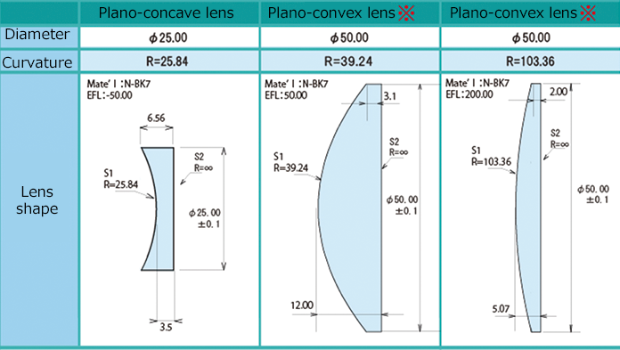
Nanoimprint onto curved surfaces Fabrication onto curved surfaces, which include lens surfaces (concave or convex)
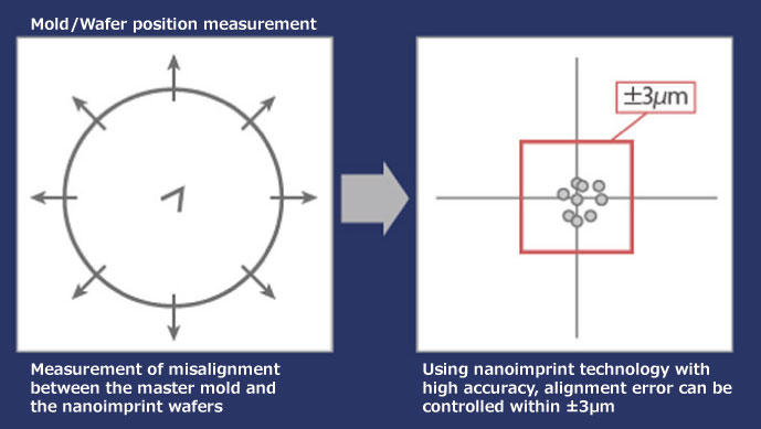
Alignment Technology
The global alignment accuracy across wafer (φ8” ) is ±3μm.
Pattern transfer with
high accuracy
For L&S with 100nm pitch, we can fabricate a pattern with precision at less than 0.1nm.
Some examples of our processing technology
Patterning onto sapphire substrates or
compound semiconductors
Uniform patterning onto substrates with some warpage or non-flatness can be done.
Patterning onto lens curved surfaces
Molding onto lens surfaces (concave, convex, and both) can be done.
Patterning onto resin
We have many patterning experiences onto resin film/substrate.
Patterning onto large-area glass
substrates
Uniform patterning at most G5 (1,100mmX1,300mm) substrate can be done.