

Example causes:
- simulation results and actual prototype results not matching
- mold not made well
- not possible to select a resin for which adequate performance is ensured
- not possible to achieve a match with etching processing
- unsure of how to appropriately inspect product quality
These are the challenges faced by many companies in mass production using nanoimprinting technology.
Nanoimprinting technology has been attracting a great deal of attention in recent years as a cutting-edge device manufacturing technology because of its ability to achieve microfabrication at a lower cost than conventional technologies, improving the performance of conventional products, and opening up new product and application possibilities.
On the other hand, since nanoimprinting appears to be a simple “stamping” technology, there are many cases in which simple imprinting equipment is introduced and then abandoned for mass production after a trial and error process.
Nano-imprinting technology is a young technology that has only been in practical use for a short time.
Many companies are adopting it in the same way as they do for mass production of semiconductors, but the situation is very different from the semiconductor manufacturing process where standard process recipes are in place.
In a sense, unlike the mass production of semiconductors, which can be carried out according to a recipe, each of the processes and materials must be optimized.
For example, the selection of resin for molding.
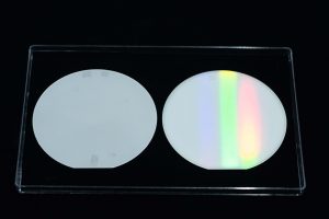
Naturally, the resin to be used must be able to form the desired film thickness uniformly and, of course, be capable of nanoimprinting and have the required characteristics (such as optical and etching characteristics). However, commercially available nanoimprinting resins are limited in variety and must be customized in most cases.
In addition to this, rules of thumb and know-how are required for each process, such as optimization of the master mold shape suitable for the imprinting process, selection of the replication resin, and optimization of the mold release process according to the shape and resin.
Moreover, there is a lot of items to consider when introducing mass production, such as residual layer control and removal, etching process, and efficient inspection process.
 SCIVAX has gathered together engineers who have led R&D and production of products at major manufacturers and research institutions in various fields (engineers in optical design, semiconductor process design and production, material design, mold design, equipment design and production, etc.) and those engineers are now tackling nanoimprint development.
Since our founding in 2004, we have devoted ourselves to nanoimprint.
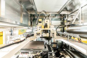
While developing nanoimprint production equipment, we are working on all nanoimprinting processes, from simulation to prototype design, mass production, and inspection. In 2018, the number of contracted development projects exceeded 1000.
The strength of SCIVAX is that, by utilizing our vast experience and knowhow, we can respond the various needs of customers.