SCIVAX can, of course, process silicon wafers, but also wide variety of other substrates including compound semiconductor wafers. Large area glass substrates can also be imprinted in our foundry with SCIVAX’s unique single-shot NIL technology.
Features of SCIVAX Nanoimprint Technology
Large Area Nanoimprint Technology
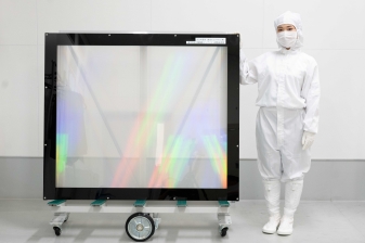
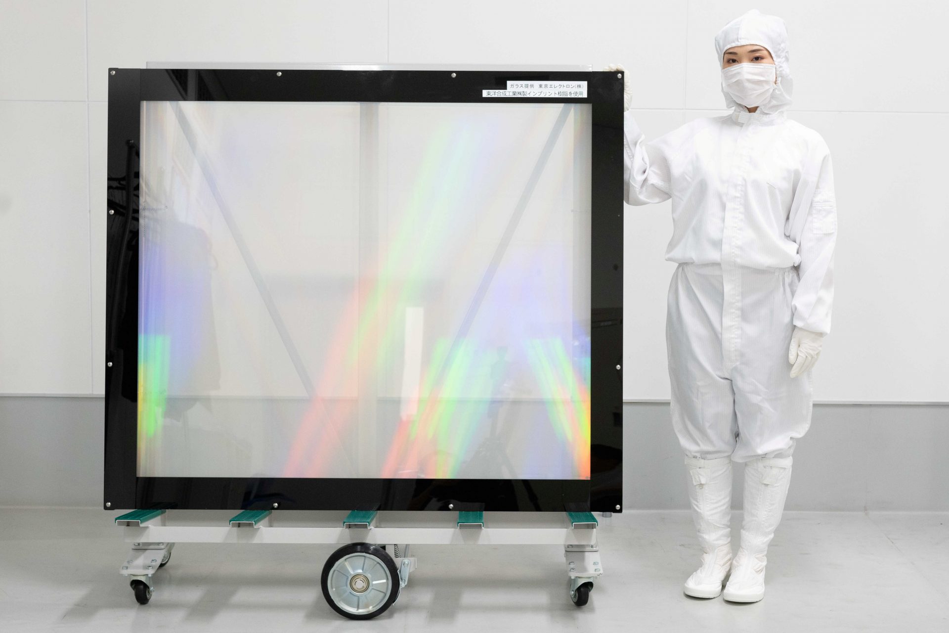
SCIVAX technology has been used in concert with other technologies to allow the first ever large area substrate single-shot nanoimprint pattern transfer.
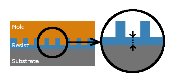
① Uniform molding technology ② Compliant molding technology for substrates with some warpage or non-flatness ③ Residual Layer Control Technology ④ Auto Mold Release Technology ⑤ Bubble Defect Reduction Technology ⑥ Particle Defect Reduction Technology ⑦ Alignment Technology
G5 (1,100 mmx 1,300 mm) Glass Panel NIL Achieved!
Available Substrates
Batch nanoimprinting is possible for various substrates ranging from silicon substrates, compound semiconductor substrates to large glass substrates.
Residual film controlled to less than 10 nm
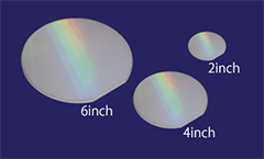
Wafer (φ2″-φ12″)
Glass (Max Size G5 = 1,100 mm x 1,300 mm)
Glass Lens
Metal Substrates
All types of resin films, sheets, substrates
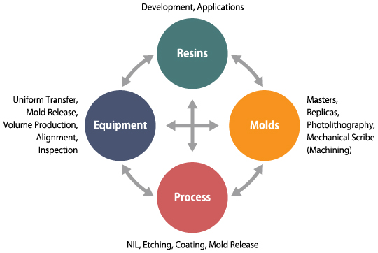
Total Process Coordination
SCIVAX has established a team of specialists with expertise in each critical technical area to deliver a total nano-foundry process capability from selection of ideal resins, to the NIL process and pre/post processing.
From pilot production to full volume manufacturing
SCIVAX offers its standard molds and molded products for sale, which can be used for R&D or basic evaluations of standard nano-patterns.
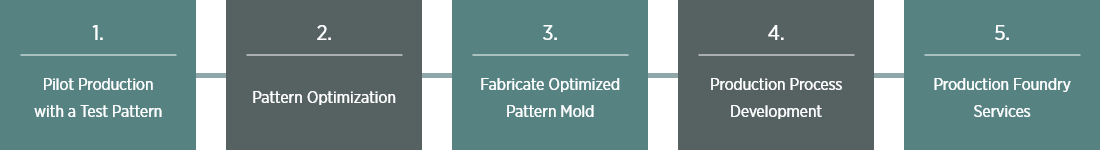
① Pilot Production with a Test Pattern
We make prototypes using test molds (ready-made molds are used). We carry out basic evaluation including principle verification.
② Pattern Optimization
Once a good result is achieved in pilot production, patterns can be optimized. We encourage customers to take advantage of SCIVAX’s optical simulation, mold fabrication know-how, and foundry services.
③ Fabricate Optimized Pattern Mold
Product prototypes are manufactured using pattern-optimized molds.
④ Production Process Development
We develop processes to achieve mass production.
Fabrication of mold for production
Customization of production systems
Quality Management Standards
⑤ Production Foundry Services
Foundry production is conducted in a high-level, well managed state-of-art facility.
Processing Examples
Substrates of various sizes and materials can be processed ◯Pattern Size: 20nm-a few hundred μm ◯Substrate: All kinds of wafers (silicon, sapphire, compound semiconductor, other), Glass Substrates, Metal Substrates, Resin Films/Sheets
Processing Anti-reflection Nanostructures (Moth-Eye) onto Films
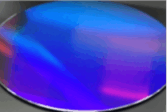
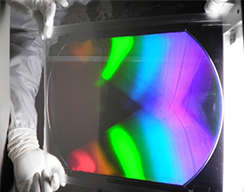
Processing of 12″ Silicon Wafers
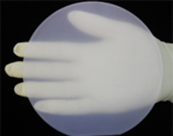
Nano-patterning of Resin Films (COP)
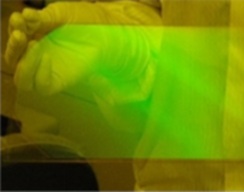
Nano-patterning of Glass Substrates
Nano-patterned 6″ Sapphire Wafer
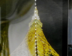
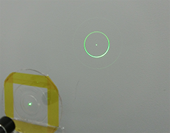
Light diffraction with diffractive optical elements (DOE)
NIL samples
SCIVAX has nanoimprinted resin film samples available for sale. The details can be found at the link below: