![]()
![]()
![]()
![]()
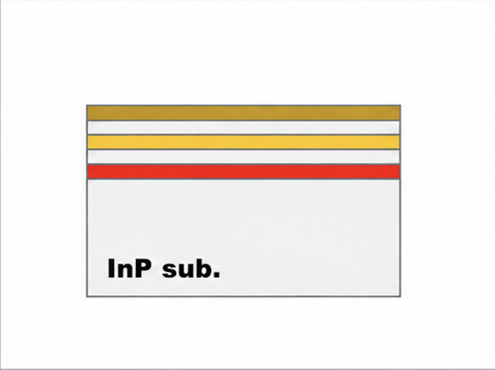
High-precision grating formation on compound semiconductor substrates such as GaAs and InP. We support lambda/4 phase shifts and wavelength tuning for DFB lasers, enabling high-throughput mass production.
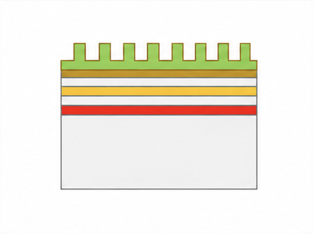
Pattern pitch is controlled at the sub-nanometer level, enabling stable formation of high-precision gratings on compound semiconductor substrates for mass production.
We support lambda/4 phase-shift gratings and chirped gratings (pitch-modulated gratings). By incorporating design information into the master mold, complex optical structures can be mass-produced with high precision and repeatability.
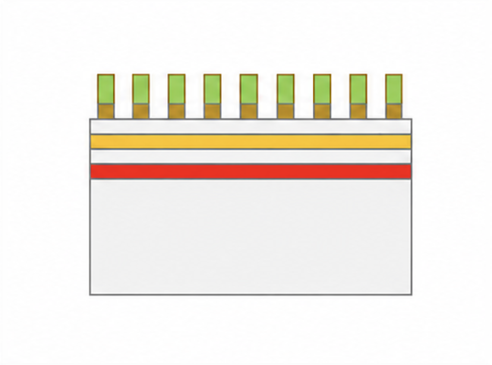
Alignment accuracy of ±1 um is possible.
Mass production is supported for compound semiconductor substrates such as InP and GaAs from phi 2″ to phi 8″.
We flexibly support everything from small-lot prototyping to mass production at the 1,000 wafers/month level, with integrated support for production launch.
| Item | Specifications / Supported Range |
|---|---|
| Supported Substrate Materials | InP, GaAs, and other compound semiconductors |
| Substrate Size | φ2″ – φ8″ |
| Pitch Accuracy | Sub-nm-level control |
| Grating Structures | Uniform gratings, lambda/4 phase shift, chirped gratings |
| Alignment Accuracy | ±1 μm level |
| Production Scale | 10 to 1,000 wafers/month (up to 50 wafers/day) |
| Lead Time (Prototype) | Test pattern fabrication: about 2 months plus evaluation / mold fabrication: 1 to 1.5 months |
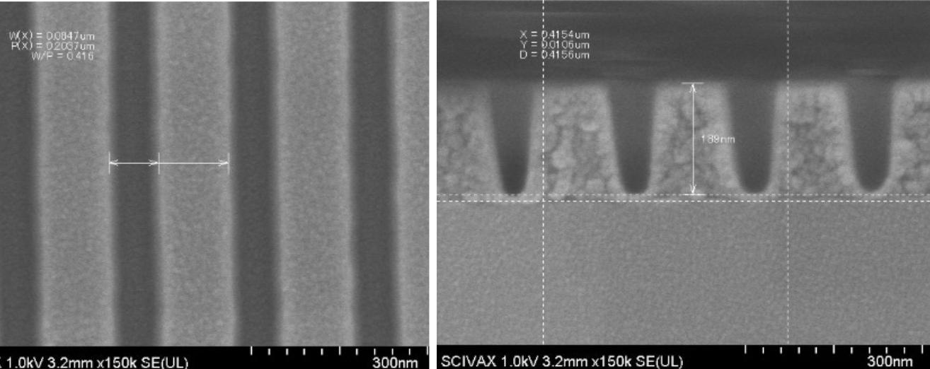
A 200 nm pitch grating is uniformly formed across the entire 3-inch InP wafer, achieving oscillation wavelength variation within ±0.1 nm.
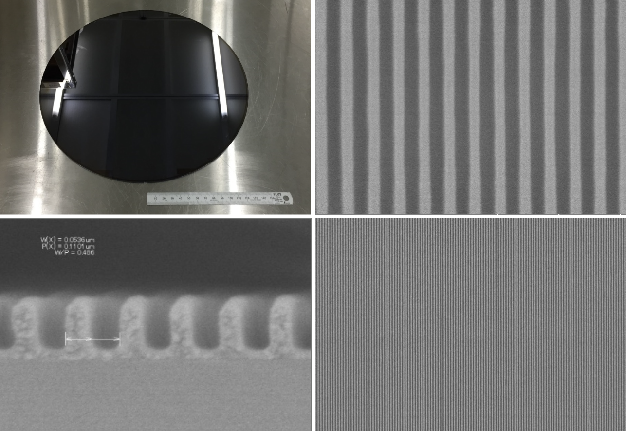
Half-pitch 50 nm L/S on a 12-inch Si wafer
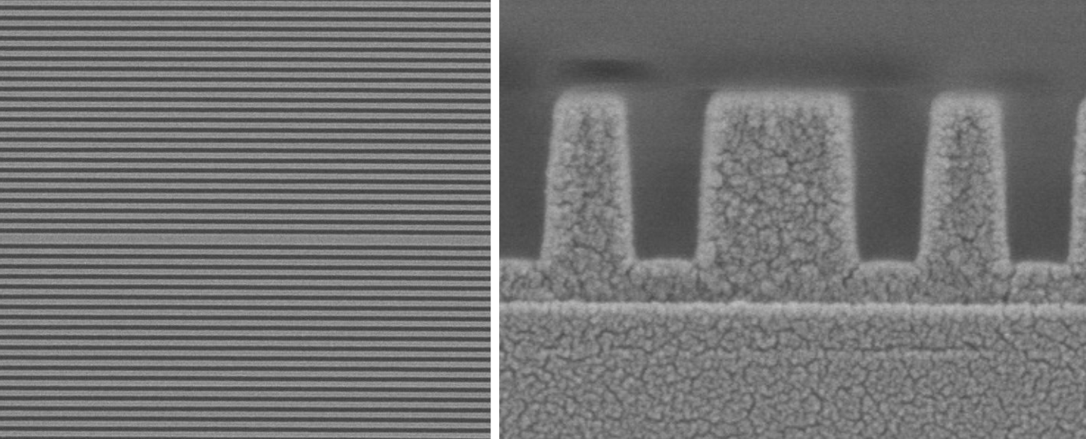
lambda/4 Phase-Shift Structure
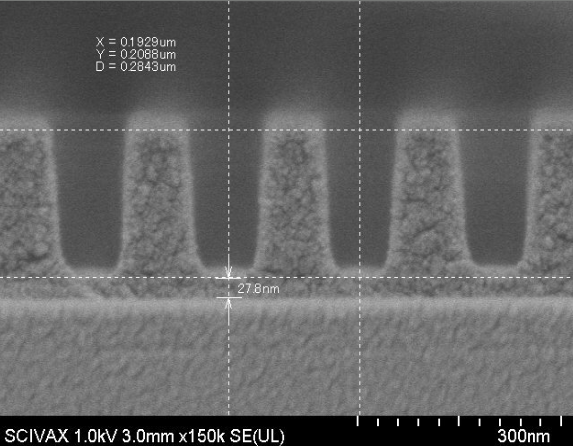
Residual layer <30 nm
We will propose a solution tailored to your specifications and production scale. Please feel free to contact us.