![]()
![]()
![]()
![]()
We support both highly reproducible design using PDKs (Process Design Kits) and custom design tailored to customer specifications. With flexible choices of materials and structures, and one-stop support from design through prototyping and mass production, we comprehensively support metalens development from R&D to practical implementation.

We provide PDKs (Process Design Kits) with pre-verified optical characteristics, allowing immediate use of process specifications, lens models, and design rules. In addition to standard PDKs, we flexibly support custom designs tailored to customer requirements, from specification studies through manufacturing.
We provide integrated support from optical analysis required for metalens design through lens design.
We support wafer sizes suited to each purpose, from R&D applications to mass production.
We respond flexibly from a single prototype wafer to mass production according to the development stage. We support production volumes of 1 to 100 wafers per month, from production launch through stable supply.
| Item | Specifications / Supported Range |
|---|---|
| Molding Method | Dry etching of inorganic materials using an NIL mask / direct molding into high-refractive-index resin |
| Supported Materials | PDK-based Amorphous Si (n=3.78) Custom support: inorganic materials such as SiN, high-refractive-index resin (n≥1.8) |
| Supported Substrates | Alkali-free glass wafers, quartz wafers 4-inch to 8-inch |
| Design | PDK-based Pitch: 385 nm / 450 nm; meta-atom diameter: 100 nm to 300 nm; aspect ratio: up to 7 |
| Operating Wavelength | PDK-based 940 nm |
| Prototype and Mass-Production Foundry Services | 1 to 100 wafers/month |
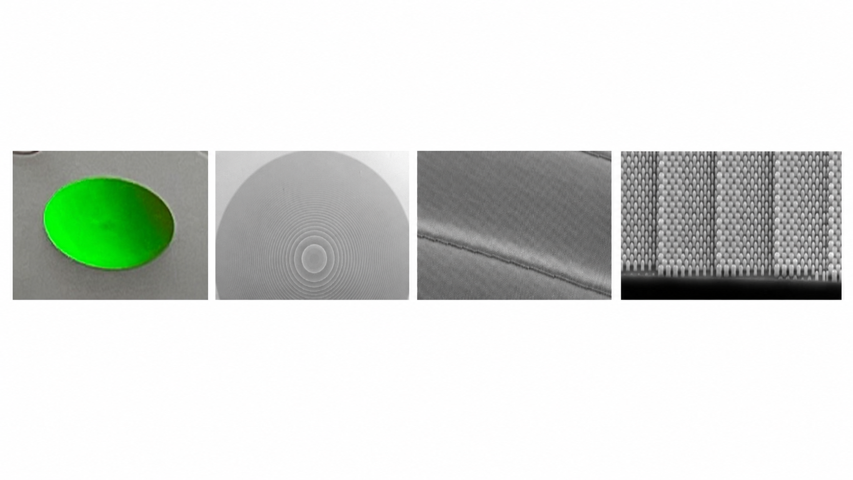
An example in which a Si substrate is etched using an NIL pattern as the mask. Pitch: 450 nm, meta-atom height: 700 nm, 12 phase steps, operating wavelength: 940 nm.
We will propose a solution tailored to your specifications and production scale. Please feel free to contact us.